2-D Materials Go Beyond Graphene
Research of 2D MXenes is prominently featured in an article in Chemical & Engineering News - bulletin of the American Chemical Society that goes in hard copy to more than 150,000 subscribers. No doubt, MXenes are at the forefront of 2D materials research.
Driven by the unique properties of ultrathin materials and their potential for new applications, researchers are crisscrossing the periodic table in search of new examples

Despite being just a single layer of carbon atoms, graphene sure can excite engineers and scientists. Unlike bulk graphite, the ultrathin material boasts flexibility, strength, and possibly enticing electronic properties for researchers to exploit in novel applications. Graphene mania crescendoed in 2010 when the material’s discovery was the subject of that year’s Nobel Prize in Physics. Since that time, researchers worldwide have been enthralled with vanishingly thin films and have succeeded in preparing a wide variety of so-called two-dimensional materials beyond graphene.
This story is about those other 2-D materials. They hail from across the periodic table and include an assortment of transition metals, carbon-group elements, chalcogenides, and others. Researchers are taking this trip through the periodic table in search of the ultrathin because, like graphene, some of the materials they’re making sport impressive properties that surpass those of their thicker counterparts.
These 2-D materials encompass electrical conductors, insulators, and semiconductors. They include chemically inert materials as well as ones that are readily modified through chemistry. And because these materials are ultrathin, they tend to be flexible and transparent, ideal features for new types of energy storage devices, high-speed and wearable electronics, and other applications.
So what exactly does it mean for a material to be 2-D?
The definition depends on whom you ask. The dozen or so scientists C&EN contacted for this story stipulate that to qualify as 2-D, the material needs to be well ordered, relatively expansive in two dimensions, and ultrathin in the third dimension—on the atomic or molecular scale. Beyond that there is little agreement.
In brief In the excitement after the isolation of graphene, materials chemists and other scientists began scrutinizing the periodic table for opportunities to make other molecularly thin materials. Driven by the chance to explore uncharted scientific territory and to discover technologically useful materials, these researchers quickly produced many examples of so-called two-dimensional materials beyond graphene.
The growing list now includes a large set of metal carbides (MXenes), a family of single-element graphene analogs (Xenes), a number of transition metal dichalcogenides, ultrathin organic crystals, and two-component nitrides.
For example, what passes as “ultrathin” can vary depending on the material and application. The graphene work that netted the Nobel Prize for Andre K. Geim and Konstantin S. (Kostya) Novoselov involved isolating one-atom-thin sheets of carbon from graphite. But researchers still consider a sample to be graphene—and a sample still exhibits some unique graphene properties—even when it is two, three, and more layers thick. In those cases, they’re just described as bilayer or few-layer graphene.
Interactive: The world of 2-D materials
Scientists have developed five groups of 2-D materials from elements across the periodic table. The key elements in each are color coded by family below.

So where do researchers draw the ultrathin line? How many atoms in thickness can a metal carbide or film of silicon be before it transitions from a 2-D material to a “thick” layered material or a coating? In general, scientists seem uninterested in assigning a strict limit to the thickness of these materials. But the thickness does matter when researchers are thinking about applications. “Mathematics is good at rigorous definitions, but this isn’t mathematics; it’s chemistry and physics,” says Boris I. Yakobson, a Rice University theoretician and materials scientist who studies 2-D materials. “It’s good to have definitions, but often, they’re not flexible enough to reflect reality.” The other gray area in defining 2-D is whether to require that these ultrathin films can be manipulated, picked up, and transferred. Two-dimensional materials can be grown via vapor deposition of precursor molecules or isolated from a multilayer crystal or flake. But a material doesn’t need to be freestanding or separable from the surface on which it was grown or derived to gain membership in the 2-D club.
Some of the materials in this story are freestanding; others are not. Not being freestanding, though, can hinder a material’s use in applications. Eventually, researchers may come up with ways to separate 2-D materials that currently cannot be freed. That kind of advance will likely open the door to developing new applications, and ultimately, new applications will continue driving this field.
One reason so many research groups focus on 2-D materials is because of the unique collection of properties the materials exhibit. For example, 2-D versions of silicon (silicene), phosphorus (phosphorene), and some of carbon’s other neighbors in the periodic table are semiconductors with band gaps and other electronic properties that, in principle, can be tuned more easily than they can in the bulk materials. That’s because those properties depend greatly on layer thickness and doping.
Adding one layer to a single-layer material significantly alters its thickness. Not so for the bulk counterpart. And because all the atoms in a single-layer film are exposed, they are all accessible for chemical modification, which can further modify electronic properties. In a bulk material, most of the atoms are buried under the surface and are inaccessible for chemical modification.
The thinness of 2-D materials also allows electric fields to leak through them and interact with other materials below them. This feature could allow researchers to control the electronic properties of those underlying layers, according to Mark C. Hersam of Northwestern University, a specialist in semiconductor devices. Scientists can use that unique electrostatic penetration to make new types of diodes, memory circuits, and other devices that would be impossible to make with bulk semiconductors, he says.

“These unique properties may lead to new and useful applications, and that is part of their appeal, but I think that’s secondary,” says Yury Gogotsi, who leads a nanomaterials research group at Drexel University. “More importantly, we’re learning to use 2-D materials as building blocks to custom make modern materials.” Gogotsi and others envision developing methods for combining, either by stacking or by juxtaposing laterally, various types of 2-D materials with distinct sets of properties to build materials with truly novel features on demand.
Regardless of whether researchers uncover truly unique properties in 2-D materials, the work is providing scientists with an exciting opportunity to trek through unexplored territory, Yakobson says.
Gogotsi agrees: “Whether you’re a five-year-old child playing with a new toy at home or a 50-year-old child playing with a new toy in the lab, it’s fun. When people see new toys, they get excited.”
These new toys can be divided into five major groups: MXenes, Xenes, organic materials, transition metal dichalcogenides, and nitrides. Some groups have many members; others few. Some have already been used in demonstration devices, while others are still laboratory curiosities. But they have all taken researchers into the ultrathin world. The rest of the story provides brief glimpses of four of these groups. To explore all the groups and take a 2-D trip across the periodic table, go to cenm.ag/2dmaterials.
MXenes: A 2-D surprise
About six years ago, Gogotsi and Michel W. Barsoum, a materials scientist at Drexel University, were searching for ways to make high-performance lithium-ion battery anodes. The team had experience with a promising family of electrically conducting carbides and nitrides known as the MAX phases. M refers to early transition metals, A symbolizes main-group elements such as aluminum and silicon, and X represents carbon or nitrogen.
The team wanted to boost the efficiency with which Li ions reversibly insert themselves in the anodes during charging and discharging. So they tried to make room for the ions by using concentrated hydrofluoric acid to selectively remove aluminum atoms from Ti3AlC2 and other MAX phases. The process improved the materials’ performance in batteries. It also completely removed the Al layers and exfoliated the crystals into ultrathin, 2-D, graphenelike sheets of Ti3C2.
The team showed that this exfoliation process can also produce Ti2C, Ta4C3, (Ti0.5Nb0.5)2C, (V0.5Cr0.5)3C2, Ti3CN, and other materials. They named the family of materials MXenes, which is pronounced “maxenes” to deliberately rhyme with graphene. The researchers have now prepared nearly 30 MXenes, and many more have been predicted (Nat. Rev. Mater. 2017, DOI: 10.1038/natrevmats.2016.98).
Many research groups are studying these 2-D materials, but the Drexel scientists remain at the forefront. They have devised a method for making MXene-polymer composites that are electrically conductive, strong, flexible, and durable—ideal properties for electrodes in energy storage and wearable technology (Proc. Natl. Acad. Sci. USA 2014, DOI: 10.1073/pnas.1414215111). The Drexel team has also demonstrated that MXenes can serve as lightweight, inexpensive shielding materials to protect cell phones and other devices from electromagnetic interference (Science 2016, DOI: 10.1126/science.aag2421). They’ve also recently started making 100-g batches of MXenes with a custom-made reactor.
Xenes: Elements go solo
Carbon isn’t the only element that can form ultrathin, monoatomic sheets. In the past few years, elements that are clustered in the periodic table near carbon (B, Si, P, Ge, and Sn) have jumped onto the 2-D stage. Scientists refer to this family collectively as Xenes, where X represents the name of the element and “ene” comes from graphene. These materials, which include borophene, silicene, phosphorene, germanene, and stanene, all share a buckled or corrugated shape—unlike graphene’s flat sheets—and sport atoms arranged in a honeycomb lattice. Silicene, phosphorene, and borophene are the most studied of the family.
“Whether you’re a five-year- old child playing with a new toy at home or a 50-year- old child playing with a new toy in the lab, it’s fun.” —Yury Gogotsi, Drexel University
Silicon is used in bulk throughout the electronics industry. But researchers in the U.S. and Italy showed that the element can also be useful in its 2-D form. The team grew a 2-D silicene layer on silver and capped it with a protective layer of alumina. The researchers used the single layer of silicon atoms as the channel in a field-effect transistor, which shuttles charge from the source to the drain electrodes (Nat. Nanotechnol. 2015, DOI: 10.1038/nnano.2014.325).
Phosphorene could also be useful for making fast electronics because of its high charge mobility. But the material degrades upon exposure to air, thwarting efforts to use it. Northwestern’s Hersam came up with one way around the problem. His group protects the material by treating flakes of black phosphorus, the starting material from which researchers isolate ultrathin phosphorene sheets, with a solution of a benzenediazonium derivative that passivates and protects the material (Nat. Chem. 2016, DOI: 10.1038/nchem.2505).
 Unlike other materials in this group, borophene has metallic character, making it potentially useful for connecting elements in circuits and acting as a transparent conductor. This Xene made its debut when two research teams used vapor deposition methods to grow one-atom-thick boron films on metals (Angew. Chem. Int. Ed. 2015, DOI: 10.1002/anie.201509285; Science 2015, DOI: 10.1126/science.aad1080). But to use borophene in applications will require separating the material intact from its support, something that has yet to be demonstrated.
Organic materials: Carbon moves beyond grapheneIt’s not just single elements, or combinations of a few elements, that can enter the 2-D world. Multielement organic molecules also form ultrathin materials.
The richness of organic chemistry offers a unique opportunity to customize the properties of these organic 2-D materials to make chemical and biological sensors, chemically selective membranes, and electronic devices. But forming these 2-D crystals is challenging because of covalent bonding between layers.
One solution has been to exfoliate covalent organic frameworks (COFs), which are crystalline porous polymers. Sonicating COFs thins them, but how thin they get depends on the strength of the bonding within a single layer versus the strength of the bonding between adjacent layers. If the interlayer bonding is stronger, the COFs resist thinning. Common boronate-linked COFs tend to do this. But as Northwestern’s William R. Dichtel showed, sonicating hydrazone-linked COFs in dioxane and other common solvents yields bulk quantities of few-layer 2-D crystals (J. Am. Chem. Soc. 2013, DOI: 10.1021/ja408243n).
A. Dieter Schlüter of the Swiss Federal Institute of Technology (ETH), Zurich, demonstrated a different approach and applied it to a related material—metal organic frameworks (MOFs), which are porous crystalline materials composed of metal ions joined by organic linkers. His team prepared a series of ultrathin crystals made of tri- and hexa-functionalized terpyridine-based groups joined by Zn2+ ions. The researchers then selectively exchanged the zinc ions with Fe2+, Pb2+, and Co2+, thereby making a new set of 2-D MOFs (J. Am. Chem. Soc. 2014, DOI: 10.1021/ja501849y).
Transition metal dichalcogenides: Scaling up
Numerous research groups have demonstrated that ultrathin layers of transition metal dichalcogenides such as MoS2 and WS2 can serve as key circuit components in fast electronics. But methods to make the thin films tend to be laborious and yield just tiny quantities of material.
To sidestep the slow production, Cornell University’s Jiwoong Park used Mo(CO)6 or W(CO)6 as precursors in a chemical vapor deposition process to form films of MoS2 and WS2, respectively, that were only three atoms thick but covered an area of about 65 cm2 (Nature 2015, DOI: 10.1038/nature14417). The films were high enough in quality to be used in field-effect transistors.
And last year, Northwestern’s Hersam and coworkers reported a low-cost method for separating single- and bilayer ReS2 through liquid-phase exfoliation based on ultrasonication followed by ultracentrifugation (NanoLett. 2016, DOI: 10.1021/acs.nanolett.6b03584).
Source: http://cen.acs.org/articles/95/i22/2-D-materials-beyond-graphene.html


 Highlights
 We are excited to share that our Carbon-Ukraine (Y-Carbon LLC) company participated in the I2DM Summit and Expo 2025 at Khalifa University in Abu-Dhabi! Huge thanks to Research & Innovation Center for Graphene and 2D Materials (RIC2D) for hosting such a high-level event.It was an incredible opportunity to meet brilliant researchers and innovators working on the next generation of 2D materials. The insights and energy from the summit will definitely drive new ideas in our own development.
 Carbon-Ukraine team had the unique opportunity to visit XPANCEO - a Dubai-based deep tech startup company that is developing the first smart contact lenses with AR vision and health monitoring features, working on truly cutting-edge developments.
 Our Carbon-Ukraine team (Y-Carbon LLC) are thrilled to start a new RIC2D project MX-Innovation in collaboration with Drexel University Yury Gogotsi and Khalifa University! Amazing lab tours to project collaborators from Khalifa University, great discussions, strong networking, and a wonderful platform for future collaboration.
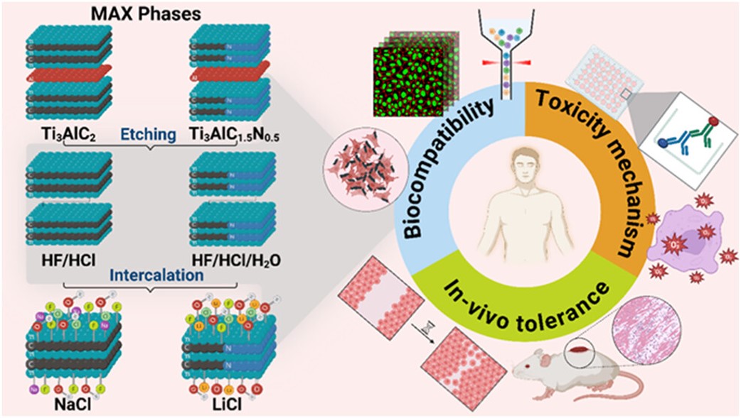 MXenes potential applications include sensors, wound healing materials, and drug delivery systems. A recent study explored how different synthesis methods affect the safety and performance of MXenes. By comparing etching conditions and intercalation strategies, researchers discovered that fine-tuning the surface chemistry of MXenes plays a crucial role in improving biocompatibility. These results provide practical guidelines for developing safer MXenes and bring the field one step closer to real biomedical applications.
 An excellent review highlighting how MXene-based sensors can help tackle one of today’s pressing environmental challenges — heavy metal contamination. Excited to see such impactful work moving the field of environmental monitoring and sensor technology forward!
 Carbon-Ukraine team was truly delighted to take part in the kickoff meeting of the ATHENA Project (Advanced Digital Engineering Methods to Design MXene-based Nanocomposites for Electro-Magnetic Interference Shielding in Space), supported by NATO through the Science for Peace and Security Programme.
 Exellent news, our joint patent application with Drexel University on highly porous MAX phase precursor for MXene synthesis published. Congratulations and thanks to all team involved!
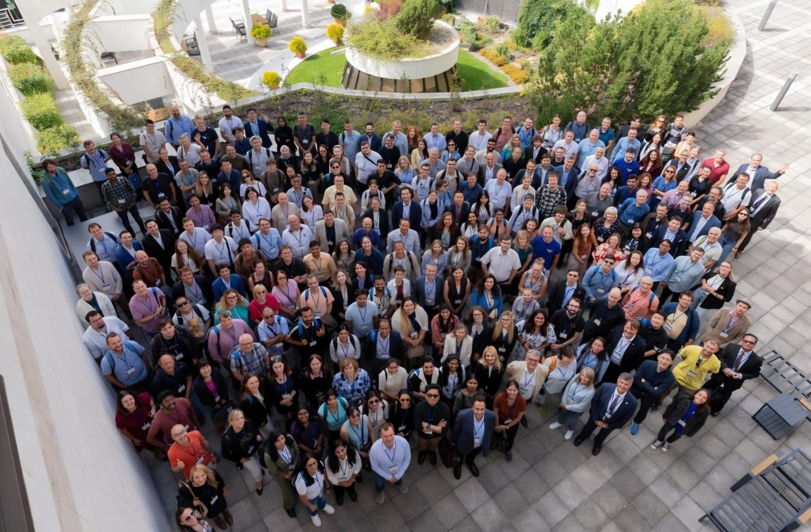 Our team was very delighted to take part in International Symposium "The MXene Frontier: Transformative Nanomaterials Shaping the Future" – the largest MXene event in Europe this year!
  Last Call! Have you submitted your abstract for IEEE NAP-2025 yet? Join us at the International Symposium on "The MXene Frontier: Transformative Nanomaterials Shaping the Future" – the largest MXene-focused conference in Europe this year! Final Submission Deadline: May 15, 2025. Don’t miss this exclusive opportunity to showcase your research and engage with world leaders in the MXene field!
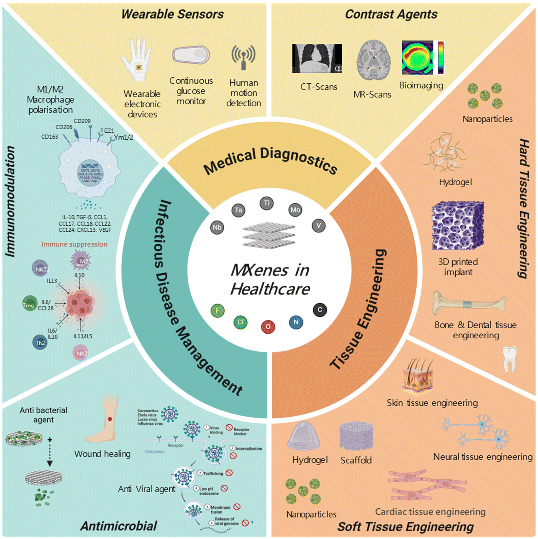 We are excited to announce the publication of latest review article on MXenes in Healthcare. This comprehensive review explores the groundbreaking role of MXenes—an emerging class of 2D materials—in revolutionizing the fields of medical diagnostics and therapeutics. Read the full article here: https://doi.org/10.1039/D4NR04853A.
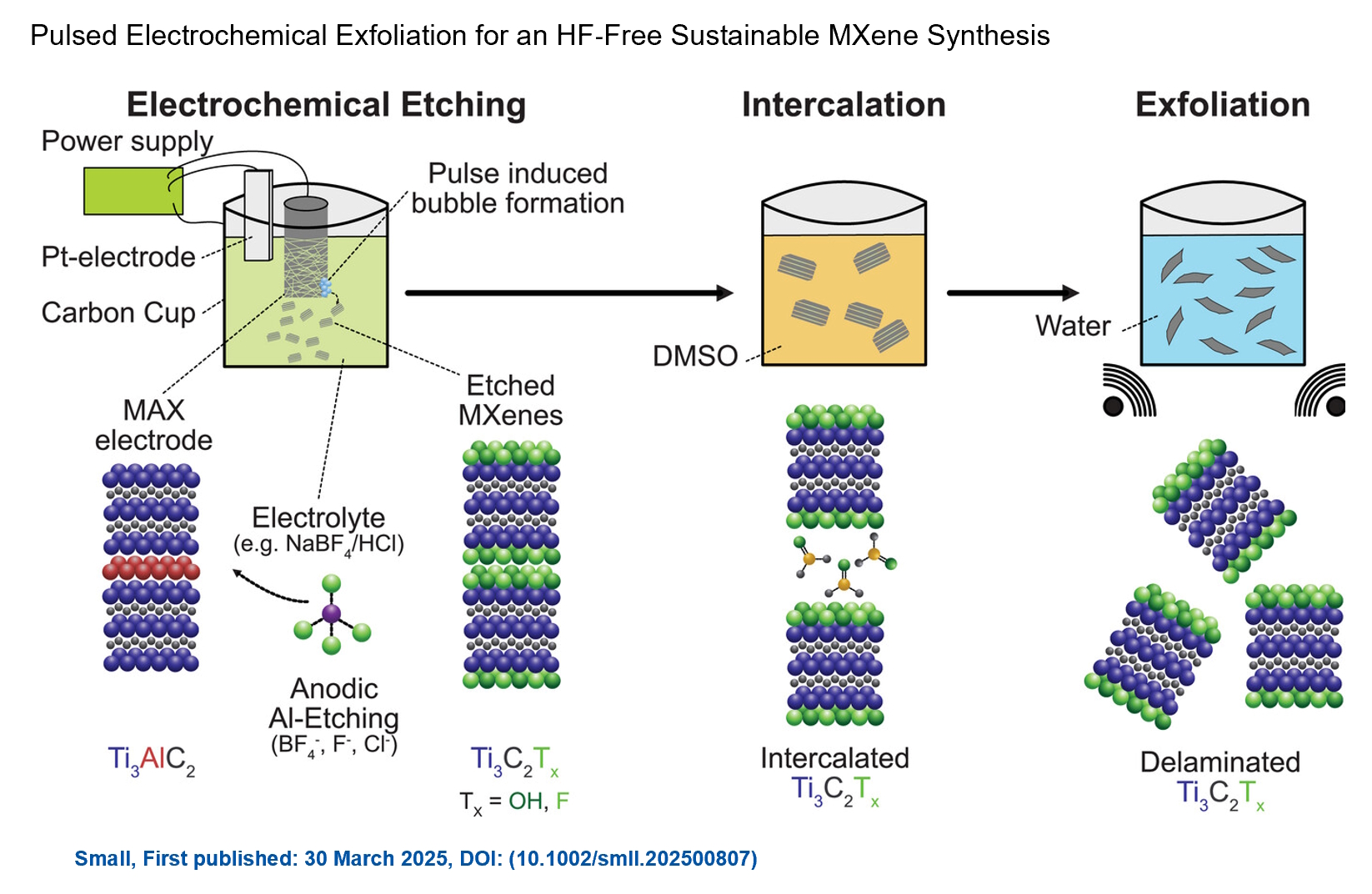 Congratulations and thank you to our collaborators from TU Wien and CEST for very interesting work and making it published! In this work, an upscalable electrochemical MXene synthesis is presented. Yields of up to 60% electrochemical MXene (EC-MXene) with no byproducts from a single exfoliation cycle are achieved.
 Congratulations to all collaborators with this interesting joint work!